3 minute read
In Part 1 of the Next Generation TV Technologies in Full View at CES 2020 article, we profiled the status of miniLED TVs and dual-cell TVs as revealed at CES 2020. In Part 2, we focus on microLED displays.
First, the term “microLED” means different things to different people. Among display technologists, the definition of a microLED is tied to the size or area of the emitter. Some think the emitter diagonal or side should be defined as less than 100 microns. Others put the dividing line at 50 microns and for AR/VR applications microLEDs need to be less than 10-15 microns.
Secondly, the LED size must also be clearly differentiated from the pixel pitch – i.e. the spacing between full-colour pixels which are made up of red, green and blue microLEDs. An LED display with a pixel pitch of 1mm can be made with either miniLEDs or microLEDs.
The third point is that microLED displays are not backlit – they are direct emissive displays with no LCD panel.
The fourth key starting point is to realise that marketing organisations have already pre-empted the term microLED. A microLED display may, in fact, use miniLEDs (typically having emitters in 200-300 micron range) or microLEDs (size depending upon what definition you like). In other words, you have to be careful to ask the right questions to really understand what has been developed.
Fifth, manufacturing for microLEDs is quite different from miniLED manufacturing. miniLEDs can use most of the same techniques that have been employed with larger-sized LEDs to make LED video walls for years. It is the size of the emitter and the package the emitters are packaged in that gets smaller, adding a need for more precision in the manufacturing process. True microLEDs require a different manufacturing process as they must often be separated from their sapphire substrate and transferred in vast qualities at rapid rates with high accuracy. This has spawned an entire industry that is developing dozens of different ways to do this. As a result, it is still early days for microLEDs as there is no clear consensus on the best manufacturing methods to achieve the desired quality displays at the needed price points.
Finally, microLED manufacturing for AR/VR applications will be different than applications with larger-sized displays. When microLEDs are fabricated, they have a tight pixel pitch on the 4” to 8” wafer. With larger, direct view displays, the pixel pitch is much bigger (0.6mm on up). As a result, a “mass transfer” manufacturing technique must be developed to spread out the wafer-scale pitch to the display-scale pitch. Typically, smaller modules 6”x6” to 12”x12” are first constructed with the mass-transferred microLEDs. These are then assembled into cabinets. Displays are built by assembling a number of cabinets in a variety of sizes and shapes.
With AR/VR, the pixel pitch of the display (5-15 microns) will be similar to the size of the emitter (1-15 microns) so no mass transfer step is needed.
Large-format microLED displays can be very bright, have a wide dynamic range and a very wide colour gamut along with a very long lifetime. In many ways, they are the ultimate display solution. Current challenges include cost and heat.
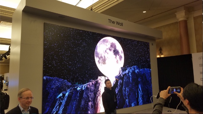
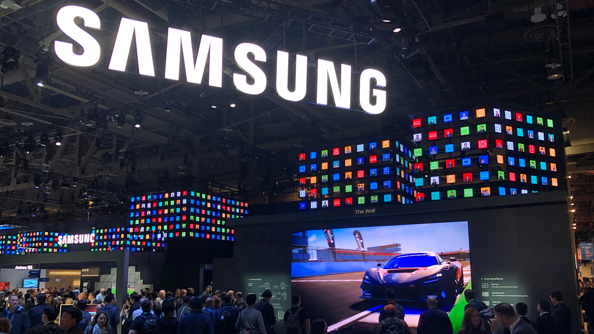
Okay, with that background out of the way, we are ready to better understand what is happening at CES. Samsung has been a leader in microLEDs, having first introduced The Wall at CES 2018. While this is available to well-heeled homeowners, it will mostly be a commercial product until prices come down. At CES 2020, Samsung doubled down on microLEDs, announcing it would expand the standard sizes it will offer to include 75”, 88”, 93”, 110”, 146” in 4K resolution and 150 and 292” in 8K resolution. These will apparently be offered with a number of TV functions and processing similar to what can be had in their high-end QLED TVs.

Sony’s Crystal LED display is, in fact, a microLED solution as well. This was shown at CES but there were no new announcements regarding plans for 2020.
Konka had two large impressive microLED solutions at CES as well. One was a 236” 8K display with a 0.68 pixel pitch and 2000 nits luminance. A second was a 118” 4K display with the same pixel pitch and luminance. Konka said these will be commercialised in China in 2020 and will likely include TV-like functionality and a 5G interface. The even offered some pricing: $1.25M for the 8K and $240K for the 4K.
LG Electronics showed a 145” 4K microLED prototype that used LEDs smaller than 50 microns. TCL showed a 132” 4K microLED prototype with 1500 nits luminance. And Planar/Leyard, a big player in commercial LED video walls, says they will set up a new TV division in China for microLED displays. They showed a 216” 8K display with a 0.6mm pitch and a 135” 4K display with a 0.7mm pitch.
microLEDs displays are coming but will mostly be a professional/commercial product for a few years. But if manufacturing issues are solved, they could start to become consumer products. This will be good news for consumers.
As this article points out, there is much innovation underway in the display ecosystem that will continue to drive the market forward.
Tags: Technology

RedShark 2020 @ All rights reserved.

Comments