3 minute read
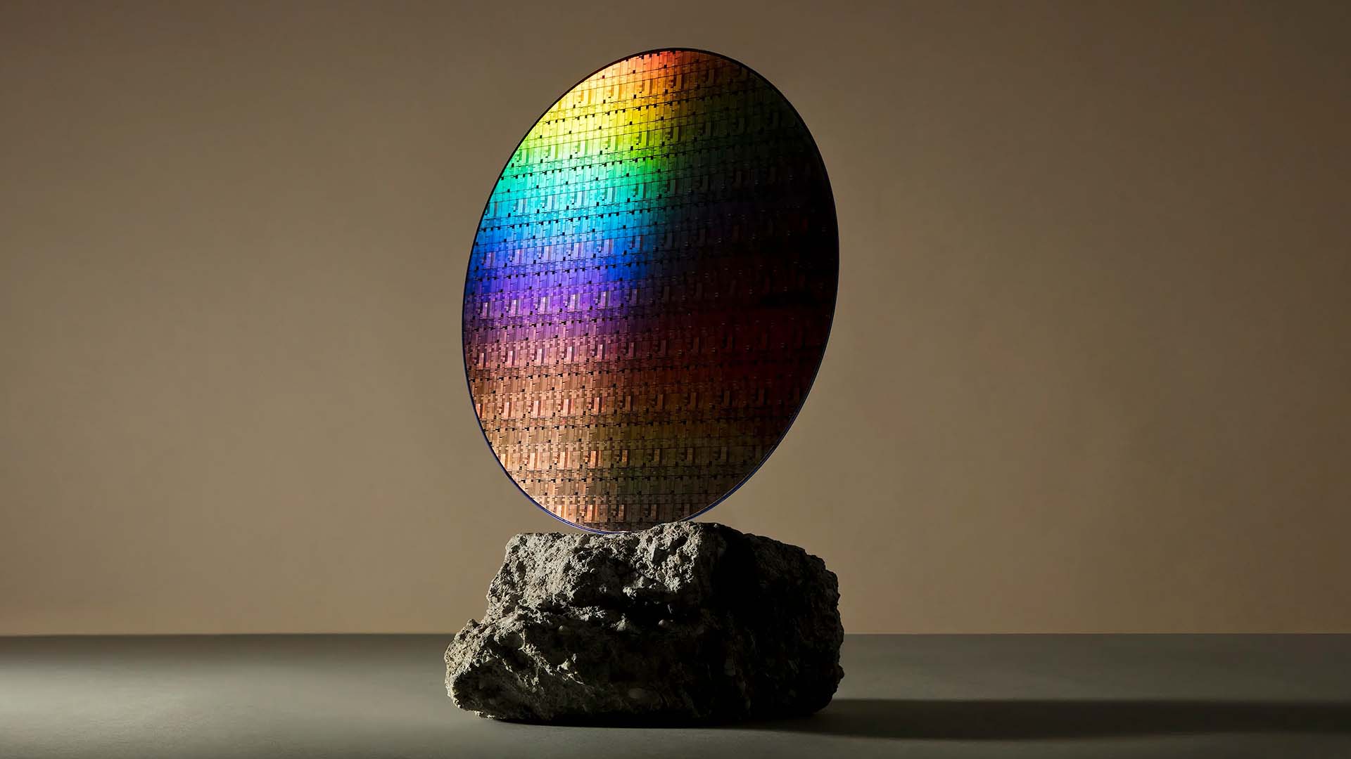
A collaboration between Samsung and IBM has produced a revolutionary new chip design, called VTFET, that could preserve the idea of Moore's Law for some time to come.
When cities run out of space, they start figuring out ways to build skyscrapers, which is why Manhattan residents don't so much have an address as a coordinate in three-dimensional space. As we'll see, that's an analogy some surprisingly far-reaching parallels with IBM and Samsung's new collaboration - a new kind of transistor intended to make microchips more compact. Or lower power consumption - or both. Or something. Let's find out.
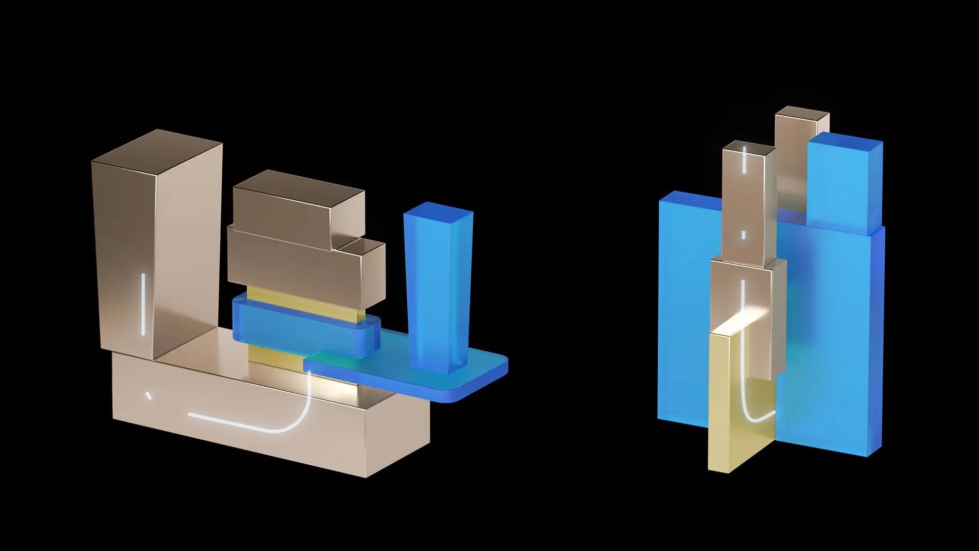
The concept is simple enough, though it's worth being clear up front that the technological challenges of working at extremely small scales are not necessarily instinctive. At the most basic level, though, the innovation we're discussing here is called VTFET, and contrasts with the more established finFET design which is probably in the computers of many of the people reading this, whether that's a laptop, a workstation or a phone.
The new approach involves stacking up the component parts vertically as opposed to horizontally, with some other layout changes that mean not only is the footprint smaller, but the likelihood of the transistor to leak current to those around it is reduced to the point where traditional isolation barriers, which waste space, become less necessary. This is the difference between the minimum feature size (approaching a few nanometres in mainstream designs) and the gate pitch, which is generally many times larger.
It's not quite clear whether the main aim of this is to pack more transistors into a smaller space, or to cause those transistors to consume less energy; possibly the answer is optionally either, or a bit of both. The pitch is that it will reduce the power consumption of cellphones to the point where a battery might last a week, although that's the sort of phraseology that's easily picked from the a refrigerator magnet set, designed to help modern public relations people say the right thing about fundamental technologies that might otherwise seem a little remote to nontechnical people.
In reality, VTFET is a very general innovation in microchip design which might help all kinds of things - thermal handling in graphics cards, CPUs in laptops - and if it's being specifically linked to cellphones, that's probably got more to do with the vast and tempting scale of the cellphone market than any specifically cellphone-relevant characteristics of the technology.
The idea that's being pushed hardest, though, is that the increased density will allow Moore's law to be maintained. It's not stated formally often enough, but what Intel and Fairchild founder Gordon Moore actually proposed was that the number of transistors on an integrated circuit will double about every two years. Making them smaller is likely to make that more practical, although there are some fairly complicated and non-intuitive reasons, things like parasitic resistance and capacitance, which can make theoretical gains difficult to realise in full.
There is also the reality that doubling the number of transistors doesn't necessarily double the performance of the CPU, at least not in all circumstances. Since the end of the 90s, we've relied largely on increased transistor count to increase core count, as opposed to wildly faster clock speeds. Writing code which takes best advantage of multi-core CPUs is still a developing art and works better for some kinds of job than others. Still, the ability to pack more in, and run it for less power, can be no bad thing in the end.
Strategically, things are a little more complicated. It's becoming abundantly clear that, even if Intel gets its 7nm process to work, x86 CPUs will struggle to match the power economics of RISC-based ARMs, in the form of every cellphone ever made, Apple's M1 series, and various server CPUs. It would be easy to think that something like VTFET is exactly the shot in the arm that Intel might need to bring its CPUs into a more competitive position. The thing is, most real world ARM devices, including Apple's feted work, are finFET-based designs too; any promise VTFET holds for any kind of integrated circuit applies just as well to the big ARMs as anything else.
VTFET is a laboratory proof-of-concept at the time of writing, and clearly some way from appearing in a product. Still, if the big question of the early 2020s is the future position of x86 CPUs and Intel as a company, this new development doesn't make the result any easier to predict specifically because it could work for almost any manufacturer willing to pay for access to it, which would still leave Intel lagging. With any luck, the much-vaunted benefits of free market capitalism should see significant effort by all involved to outdo each other, pushing R&D money where it needs to go. Without that luck, the much-vaunted benefits of free market capitalism might just keep Intel spending money bolstering its own stock price, as if you can render a Maya scene on a NASDAQ code.
Tags: Technology CPUs microchip

RedShark 2020 @ All rights reserved.

Comments