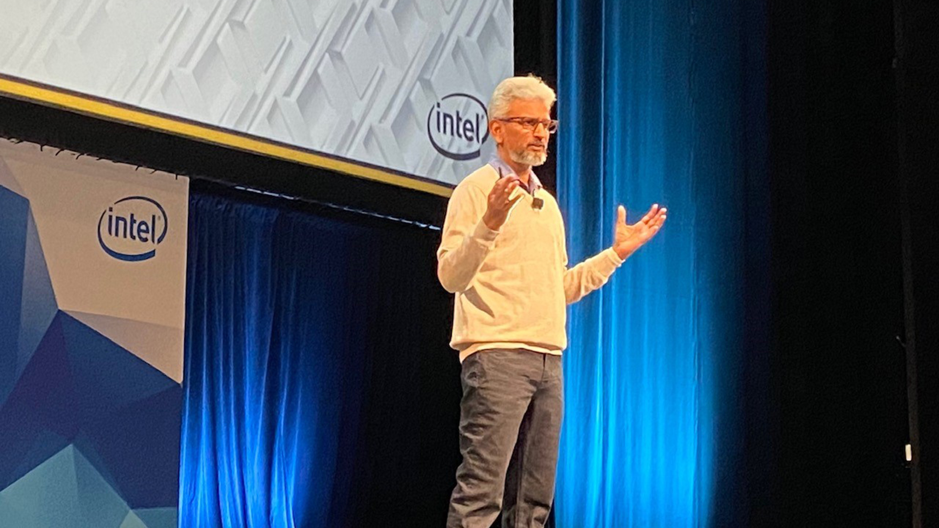

At Intel’s HPC Developer conference, Raja Koduri revealed information about the Xe graphics computing architecture that he’s been working on.
There will be a version for mobile applications under the Xe LP brand, high performance for the gaming and datacenter/AI market called Xe HP, and an excascale variant called Xe HPC for supercomputing.
Since the conference is for HPC, that was the focus of Raja’s presentation, but they’re the same architecture scaled to fit each application, rather than different architectures.
The Xe GPUs will be manufactured on 7nm, making the Xe Intel’s first 7nm parts. Using the Foveros and EMIB packaging, Intel will be able to integrate the Rambo Cache, a new scalable memory fabric is designed to allow the Xe to sustain its peak FP64 throughput, and is shared between the CPU and GPUs. Using Intel’s Foveros and EMIB packaging will enable Intel to integrate several Xe compute units and Rambo Cache into a single chip carrier.

Each Aurora compute node will consist of a pair of Sapphire Rapids Xeon processors based on the 10nm++ Willow Cove architecture and six Xe HPC GPUs, each of which will incorporate 16 (yes, 16) GPU chiplets onto a single interposer along with a Rambo Cache and a large High Bandwidth Memory buffer, and connected to each other using a Compute Express Link (CXL) based Xe Link connection.
While Ponte Vecchio will be launching in 2021 using Intel’s 7nm process, the low power and enthusiast models will be launching in 2020 using Intel’s 10nm process to compete with AMD’s RDNA2 and nVidia’s Ampere.
Tags: Technology


Comments