3 minute read

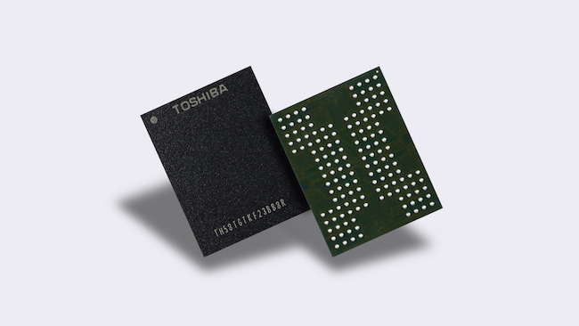
 Toshiba's QLC 3D Flash Memory
96-layer 3D NAND flash using a technology called BiCS4 means that we could probably see 1.5TB NAND-powered SSDs in about a year.
You may recall that WDC (Western Digital Corporation) became partners with Toshiba in the silicon chip business after WDC bought SanDisk, and this is the central point about something curious that happened recently in the world of press releases.
On the 27th June WDC announced the first use of 96-layer 3D NAND flash using a technology called BiCS4 (Bit Cost Scaling) which follows on from 64-layer BiCS3.
The following day, on the 28th June Toshiba issued its own Press release which covered very similar points in a slightly different way.
In a typical 50:50 partnership you might expect identical wording with just a change in the corporate letterhead. There is an element of Kremlinology here as Toshiba is trying to sell its chip business to cover its awful financial problems and therefore has fairly short term interests, while WDC is looking to the longer term. Both press releases are brief and I found it interesting to stitch them together to get the full picture.
3D NAND has a number of uses but the ones of keenest interest to readers of RedShark News are SD cards and SSDs.
In 2015 Toshiba and SanDisk announced 48-layer BiC2 3D NAND which is 2-bits per cell MLC NAND at 128Gb/16GB and 256Gb/32GB density. This flash has been used in a handful of products while the first generation of BiCS was not put into mass production. In May 2017 Toshiba demonstrated BiCS3 in a Toshiba XG3 SSD and Toshiba/WDC now say they expect ‘production of 64-layer TLC NAND will be higher than any other industry supplier in calendar year 2017’.
In that context it is worth noting that Intel has launched a model of SSD called 545 that uses 64-layer TLC NAND so on the face of it BiCS is currently losing out to Intel. Having said that Intel 545 appears to be more of a demonstration of intent, rather than an item in mass production but there is no denying that BiCS3 is in its early days.
This makes the announcements about BiCS4 seem a tad premature as the first 96-layer NAND will be sampled in H2 2017 with production starting in 2018 using three Fabs at Yakkaichi Operations in Japan. The third of these Fabs, Fab 6, is scheduled to open in Summer 2018 so it is anyone’s guess exactly how much 96-layer NAND will actually be produced in 2018.
The other question mark lies over what sort of NAND will be produced using BiCS4. The easy and obvious answer is that Toshiba/WDC will simply stack up the existing 3-cell TLC, initially 256Gb/32GB, then 512Gb/64GB and ultimately 1024Gb/128GB which means Toshiba/WDC will be able to produce SSDs that are double the capacity of existing drives. Greater density allows higher capacity while costs are kept under control, which is good news. The better news is that once 96-layer stacking is sorted we can expect Samsung, Intel/Micron and Toshiba/WDC to move on to the next technology (128-layer?) and onwards, ever onwards in a steady progression.
Perhaps the biggest news in this pair of Press releases is that Toshiba/WDC is also talking about using BiCS4 for QLC NAND which stores 4-bits per cell. This appears to have 50 percent greater capacity than TLC and we expect BiCS4 will be used for 512Gb/64GB TLC and 768Gb/96GB QLC. In time you would hope 1,536Gb/192GB would be on the roadmap.
Reading data from NAND requires that you interrogate the voltage level that has been set in each cell. Single-bit SLC is easy as the voltage is either high or low which gives you a binary 0 or 1.
2-bit MLC has four states and three dividing lines so you have to exhibit some care to distinguish between values that lie close to a dividing line.
TLC is 3-bit which in binary terms means it has eight states and seven dividing lines so you have to read and write more slowly, apply more error correction and take even more care.
QLC takes this a stage further so you now have 16 states per cell with 15 dividing lines and the increments between each state are tiny.
Another factor with SLC, MLC and TLC is that the cells effectively wear out over time with each P/E (Program-Erase) cycle. As you move from SLC to MLC and TLC the narrower dividing lines between each programmed state has a major impact on the number of P/E cycles the chip can endure.
SLC is typically rated at 100,000 cycles, MLC at 3,000 cycles and TLC at 1,000 cycles. QLC had been expected to last about 100 cycles before the cells are scrapped, which suggested that QLC would be fairly hopeless for SD cards and general purpose SSDs. The obvious market for QLC SSDs appeared to be archives where files are written once (or a few times) and then read many times.
The good news is that Toshiba/WDC has answered the specific question about QLC P/E endurance and has said it is good for 1,000 cycles which is the same as TLC. If this figure is confirmed it means that QLC NAND will be fit to use in regular SSDs and SD cards.
So the messages here are that Toshiba/WDC are stacking their NAND chips higher, which should lead directly to 1.5TB SSDs in about a year. Some time after that we can expect further increases in capacity if QLC NAND comes to fruition.
Tags: Technology

RedShark 2020 @ All rights reserved.

Comments