
4 minute read

 CPU architecture is approaching some fundamental limits
We've grown used to CPUs having smaller and smaller features - and hence being more powerful with each generation - but this trend might be about to end as it starts to butt up against some fundamental laws of physics.
The ability of truly pocket-sized cameras to record incredible video is reliant on running technology at the very limits of its capability. We've been using computer CPUs at those limits for years, though; witness the ever-increasing scale and sophistication of the heat-dissipation devices we're required to clamp on top. While power consumption has risen alongside capability, it hasn't risen nearly as fast. Something else has changed.
Let's start with an example. Modern workstation CPUs run at perhaps 3,000MHz. That is, at the very least, hundreds of times faster than those of a few decades ago. The Motorola 68000 CPU in a Sega Megadrive (Genesis, Americans) ran at a bit more than 7MHz and only dealt with, in general, 16 bits of data at a time, compared to the modern CPU's 64. There are all kinds of considerations to make when comparing CPUs, but that makes the modern workstation between 500 and 2000 times more capable, no matter what other sophistications are involved.
The workstation, however, doesn't draw between 500 and 2000 times the power, even though it's got a lot going on other than the CPU. The actual numbers are something like 20:1, where a Megadrive (er, Genesis) pulls perhaps 10-15 watts and a modern PC might idle at a bit less than 200 – more for a big workstation, but not 2000 times more. Clearly, the power-to-performance ratio has improved very, very dramatically and it's this ability to do a lot of work without flattening the batteries too quickly (and without creating a large cloud of smoke) that's made things like Blackmagic's superb Pocket Cinema Camera possible.
 Making things smaller on microchips makes low power consumption possible and facilitates things like the pocket camera.
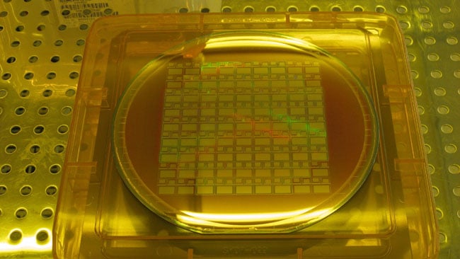
For that matter, that sort of ability has made more-or-less everything we currently use possible and the way it's been done is crafty in the extreme – we make things consume less power by making them smaller. This will be familiar to anyone who's seen CPUs talked about in terms of their minimum feature size, which is usually in nanometres. 14nm features have recently become common in CPUs, with the first devices shipped by Intel in 2014. Yes, these are the same nanometres that we use to refer to wavelengths of light, which is usually in the hundreds of nanometres for the sort of things we can detect with cameras and our eyes. Blue light, at the shorter end of the spectrum, is often around 350nm in wavelength, 25 times bigger than the features on a modern CPU.
 Semiconductor manufacturing techniques have massively improved power consumption versus performance,
mainly through making things very small.
Computer processors have small parts. What isn't clear is why smaller features allow devices to use less power and thereby go faster and do more without creating a small but spectacular explosion. Understanding this requires some knowledge of how the transistors that form the CPU work. In the broadest possible sense, each of them is formed by layering materials together to form input, output and control regions (called the source, drain and gate, depending on the exact type of transistor involved). Unfortunately, creating layers of conductive and insulating materials also creates capacitance, a sort of electronic springiness, and that capacitor has to be charged up (er, stretched) in order to turn the transistor on. This takes power, so every time we switch a transistor in a CPU, a small amount of electricity is transformed to heat.
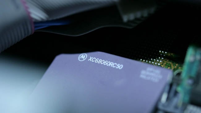 This Motorola 68060 processor from the mid-90s doesn't even need a heatsink.
This would be OK, except that a lot of modern CPUs have two to four billion transistors, so the total thermal load is high. Make the transistor smaller, though, and while it behaves, broadly speaking, in the same manner, the capacitance goes down and the amount of power required to switch it on-or-off is consequently reduced. Since the transistor is made of a series of stacked layers, its area is equal to its dimensions multiplied together, so reducing the minimum feature size a bit reduces the area (and the capacitance) a lot. This is why CPU manufacturers, such as Intel, and companies who make things like Ethernet controllers and other ancillary hardware have chased smaller feature sizes.
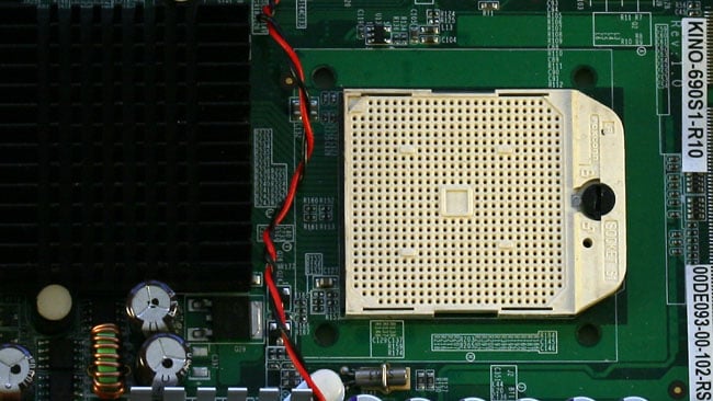 This CPU socket takes an AMD Turion processor, a device thousands of times more powerful than the 060,
but which still found use in laptops.
The problem is that, at 14nm, we're already starting to hit some fundamental limits. A single atom of silicon is about 0.2nm across, so there's only perhaps 70 of them across each feature on the device. Such small features can mean that transistors begin to conduct even when they're switched off, creating a constant background leakage of current which increases overall power consumption. The issues of manufacturing ever-smaller devices are a practical concern, too. Most semiconductors are made by photolithography, where each layer of the device is etched chemically using an etch-resistive layer that's patterned by exposure to light. The techniques used already rely on ultraviolet light of very short wavelength, because it's impossible to cast a shadow of something that's 14nm wide with light that's of a 350nm wavelength. Even beyond that, there are actually separation layers on a device which are even smaller than the headline dimension.
These are some pretty fundamental problems which stand to end a pursuit of tininess that's been ongoing since the mid-80s (when 1,000nm features were the norm). Happily, there are other ideas afoot which will allow us to both stack more complexity into the same space and reduce power consumption. Some of them are related to the techniques we've examined before, which are intended to allow designers of imaging sensors to make different parts of the device, using entirely different processes, and stack them together.
Either way, much like the difficulties with further clock speed increases, there are concerns over further process shrinks – and it's the reduced power consumption of smaller processes which have made those clock speeds possible, to at least some extent. Whether the bluer skies of graphene, photonics or quantum computing (all of which are real things and not reliant on science fiction) will save the day remains to be seen.
Graphic: shutterstock.com
Tags: Technology

RedShark 2020 @ All rights reserved.

Comments